 |
| ||||||||||||||||||||||||||||||||||||||||||||||||||||||||||||||||||||||||||||||||||||||||||||||||||||||||||||||||||||||||||||||||||||||||||||||||||||||||||||||||||||||||||||||||||||||||||||||||||||||||||||||||||||||||||||||||||||||||||||||||||||||||||||||||||||||||||||||||||||||||||||||||||||||||||||||||||||||||||||||||||||||||||||||||||||||||||||||||||||||||||||||||||||||||||||||||||||||||||||||||||||||||||||||||||||||||||||||||||||||||||||||||||||||||||||||||||||||||||||||||||||||||||||||||||||||||||||||||||||||||||
|
| ||||||||||||||||||||||||||||||||||||||||||||||||||||||||||||||||||||||||||||||||||||||||||||||||||||||
Andreas Lange
DED Feedback, Philippines
91-34-0307/2
Deutsche Gesellschaft f�r Technische Zusammenarbeit (GTZ) GmbH
|
| ||||||||||||||||||||||||||||||||||||||||||||||||||||||||||||||||||||||||||||||||||||||||||||||||||||||
Preface
Nearly two years ago - the German Development Service (DED) offered me the possibility to assist a technical college in the Philippines.
I had finished my studies in electronic engineering in Germany and had gained several years of working experience in the development of medical electronic equipment and the organization of telecommunication units.
Since I have been assigned with the Don Bosco Technical College, I have been teaching in electronics/ computer science, and have been working in the training for instructors.
One of the mayor problems I encountered was the lack of preparation time for the lessons. Many teachers are under steady time pressure because they have to serve two or more jobs in order to earn the adequate income. That gave me the idea to develop a ready-made lesson preparation for teachers.
Based on my experience and also due to the visit of many other schools I edited and compiled this Teaching Aid. I tried to integrate practice and theory which is the best way to provide a solid foundation. I hope this will support the teachers as well as it can improve the quality of classes.
Andreas Lange
Canlubang, Philippines
November
1993
|
| ||||||||||||||||||||||||||||||||||||||||||||||||||||||||||||||||||||||||||||||||||||||||||||||||||||||
Introduction
Amplifier Teaching Aid is a teaching module made for teachers. It. is a ready-made lesson preparation and not a textbook. Therefore, you (the teacher) should already have some background knowledge on analog electronics. This module gives you all the material you need to run a course in basic analog electronics.
The module is divided into lessons/ each lesson is headed by a lesson plan followed by boardscripts, worksheets, and experiments. It also contains three evaluations which you can use as tests/exams or as advanced exercises. The lesson plans are not only containing the contents of the lesson, but also gives you the objectives and suggested methods and ways to carry out the lesson.
The following informs you about the purpose of every lesson plan column:
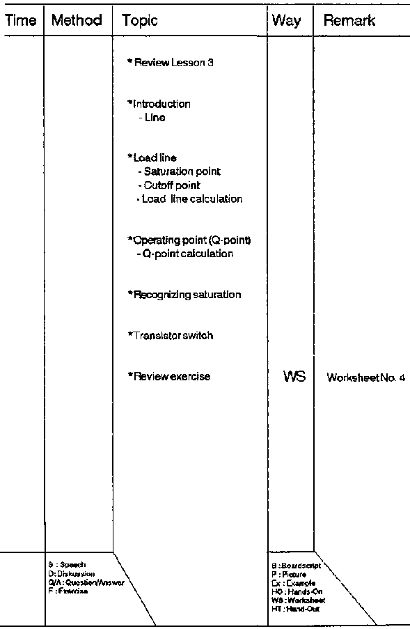
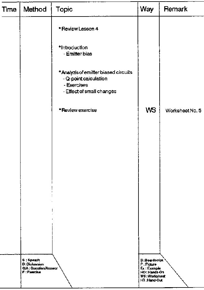
|
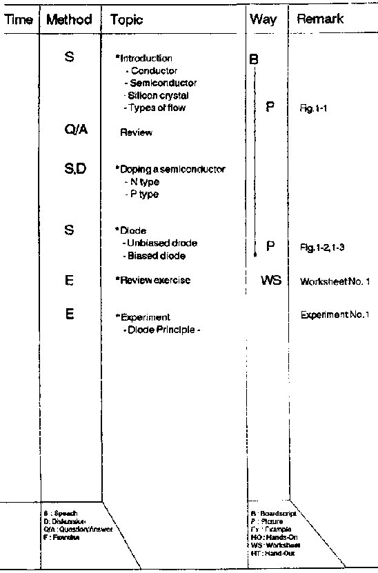
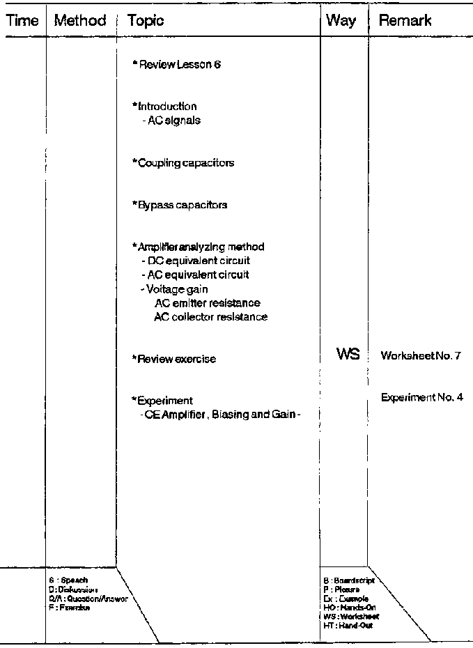
Time |
-The 'Time' column is still blank, it is up to you to decide how much time you would like to spend on each topic. The average time per lesson is approximately 90 minutes. |
|
Method |
-The 'Method' column suggests a sample of teaching methods. Lesson plan 1 and 2 are already filled up to give you an example on how to use this column. I recommend the use of abbreviations, the meaning of every abbreviation is given at the bottom of every method column. |
|
Topic |
-The 'Topic' column gives you a brief description of the contents of every lesson. Feel free to add or drop some topics. Every topic is handled in the following boardscript pages. |
|
Way |
-The 'Way' column suggests a sample of teaching tools. Lesson plan 1 and 2 are already filled up . The explanation for the abbreviation used is given at the bottom of every way column. The boardscript pages of every lesson contain examples (EX) and hands-on (HO) exercises. The HO's should be carried out by the students during the lesson. |
|
Remark |
- The 'Remark' column provides you with space for additional information. (i.e.: Where can I find the transparency/ picture which I decided to use, or: What is the filename of the demo program which I already prepared) |
This analog electronic course is designed for students with prerequisite knowledge in electronics. At least, they should know how to use Ohm's and Kirchhoff's law. Also some laboratory experience (how to measure voltage .current and resistance) is needed.
|
| ||||||||||||||||||||||||||||||||||||||||||||||||||||||
Amplifier Teaching Aid (DED Philippinen, 86 p.)
Lesson 1 - Semiconductor Review
Lesson Plan
Title: Semiconductor Review
Objectives:
- Know the difference between conductor and
semiconductor
- Able to describe N- and P type semiconductor
- Understand
the diode principle
Figure
Introduction
Conductor
A neutral copper atom has only one electron in its outer orbit. Since the single electron can be easily dislodged from its atom, it is called a free electron.
Semiconductor
Silicon is the most widely used semiconductor material. The number of electrons in the valence orbit is the key to conductivity. Conductors have one valence electron, semiconductors have four valence electrons, and insulators have eight valence electrons.
Silicon Crystals
Each silicon atom in a crystal has its four valence electrons plus four more electrons that are shared by the neighboring atoms. At room temperature, a pure silicon crystal has only a few thermally-produced free electrons and holes.
Intrinsic Semiconductor
An intrinsic semiconductor is a pure semiconductor. Intrinsic silicon acts as an insulator at room temperature.
Two Types of Flow
Flow of free electrons, flow of holes

Fig. 1-1: Types of
Flow
Doping a semiconductor
Doping increases the conductivity of a semiconductor. A doped semiconductor is called an extrinsic semiconductor. When an intrinsic semiconductor is doped with pentvalent (donor) atoms (i.e. Arsenic atoms donates one free electron to the crystal), it has more free electrons than holes.
---> N-type semiconductor
When an intrinsic semiconductor is doped with trivalent (acceptor) atoms (i.e. Baron atoms in the crystal will create a hole which is capable of accepting an electron), it has more holes than free electrons.
---> P-type semiconductor
Diode
Unbiased Diode
An unbiased diode has a depletion layer at the PN-junction. The ions in this deplation layer produce a barrier potential. At room temperature, this barrier potential is approximately 0.7V for a silicon diode.
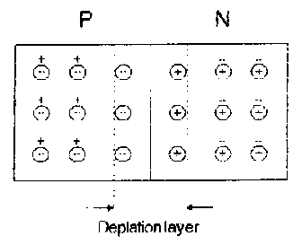
Fig. 1-2: Unbiased diode
Biased Diode
When an external voltage opposes the barrier potential, the diode is forward-biased. If the applied voltage is greater than the barrier potential, the current is large. In other words, current flows easily in a forward-biased diode.
When an external voltage aids the barrier potential, the diode is reverse biased. The width of the depletion layer increases when the reverse voltage increases. The current is approximately zero. The reverse biased diode acts like an open switch.
Breakdown
Too much reverse voltage will produce either avalanche or zener effect. Then, the large breakdown current destroys the diode.
Recap
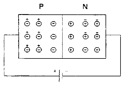
Fig. 1-3: Forward biased diode
What happens to an electron in this circuit?
1. After leaving the source terminal, it enters the right end of the crystal.
2. It travels through the N-region as a free electron.
3. At the junction it recombines with a hole and becomes a valence electron.
4. It travels through the P-region as a valence electron.
5. After leaving the left end of the crystal, it flows into the positive source terminal.
Worksheet No. 1
No. 1 How many valence electrons does a silicon atom have?
No. 2 Silicon atoms combine into an orderly pattern. What is it called?
No. 3 If you wanted to produce a P-type semiconductor which of these would you use?
Acceptor atoms
Donor
atoms
Pentavalent impurity
Silicon
No. 4 Holes are minority carriers in which type of semiconductor?
No. 5 What is the barrier potential of a silicon diode at room temperature?
No. 6 What happens to an electron travelling through a forward biased diode?
Experiment No. 1

Figure
Procedure
Increase the voltage starting at 0V up to 5V. Observe voltmeter and ammeter.
Result
__________________________________________________

Figure
Procedure
Increase the voltage starting at 0V until the ammeter show a reading.
Result
__________________________________________________
|
| ||||||||||||||||||||||||||||||||||||||||||||||||||||||||||||||||||
Amplifier Teaching Aid (DED Philippinen, 86 p.)
Lesson 2 - Bipolar Transistor
Lesson Plan
Title: Bipolar Transistor
Objectives:
- Know the structure and symbols of bipolar
transistors
- Able to calculate the current gain
- Understand how the
currents in a transistor are split

Figure
Introduction
Amplifier Principle

Fig. 2-1: Amplifier- principle
Small- and Large Signal Amplifier
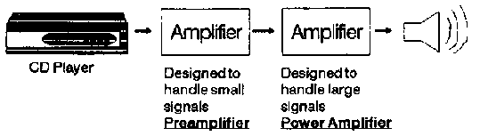
Fig. 2-2: Pre- and power
amplifier
Amplifier circuits provide power gain.
Ex: P input- = 5 mW, P output = 50 W

Transistor structures and symbols

Fig. 2-3: NPN and PNP
structure
Transistor currents
(see Fig. 2-4)
VBB forward biases the emitter diode, forcing the free electrons in the emitter to enter the base. The thin and lightly doped base gives almost all these electrons enough time to diffuse into the collector. These electrons flow through the collector, through RC, and into the positive terminal of the VCC voltage source. In most transistors, more than 95% of the emitter electrons flow to the collector, less than 5% flow out the external base lead.
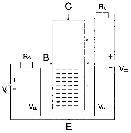
Fig. 2-4: NPN Transistor
Recall Kirchhoff's current law:
=> IE = IC + IB

Fig. 2-5: Transistor currents
Because IB is very small, for circuit analysis, we can do the following approximation:
IC is equal to IE
Current gain
Transistor circuits provide the power gain that is needed in electronic applications. They also provide voltage gain and current gain (bdc). Current gain bdc of a transistor is defined as:

Ex:
IC = 10 mA
IB = 40 mA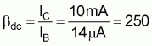
Transistor connections

Fig. 2-6: Transistor
connections
CE CONNECTION
The common emitter (CE) connection is the most widly used transistor connection.

Fig. 2-7: CE amplifier, base
biased
Base supply voltage: VBB
Collector supply voltage:
VCC
Voltage base to ground: VB
Voltage emitter to
ground : VE
Voltage collector to ground :
VC
Worksheet No. 2
No. 1 A transistor has an emitter current of 10 mA and a collector current of 9.95 mA. What is the base current?
No. 2 A transistor has a current gain of 150 and a base current of 30 mA. What is the collector current?
No. 3 If the collector current is 50 mA and the current gain is 75, what is the base current?
Experiment No. 2

Figure
Procedure
* Connect the circuit. R1 and R2 must be set for maximum resistance before power is supplied.
* Connect the power supply, adjust R1 for 10 mA base current and adjust R2 to maintain VCE at 6V, Measure and record IC in the table below.
* Repeat the measurement for every value of IB given in the table.
* Calculate the current gain (beta) for every measurement.
|
Step |
IB mA |
lC mA |
beta |
VCE volt |
|
1 |
10 |
| |
6 |
|
2 |
20 |
| |
6 |
|
3 |
30 |
| |
6 |
|
4 |
40 |
| |
6 |
|
5 |
50 |
| |
6 |
|
| ||||||||||||||||||||||||||||||||||||||||||||||||||||||||||||
Amplifier Teaching Aid (DED Philippinen, 86 p.)
Bipolar Transistor II
Lesson Plan
Title: Bipolar Transistor II
Objectives:
- Able to analyze a base biased CE
configuration
- Able to name the regions of operation in a collector
curve
- Know how to test a transistor

Figure
Introduction
Base Curve (Input)
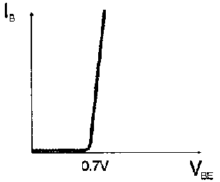
Fig. 3 - 1: Input curve, base
biased CE connection
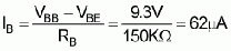
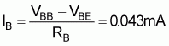
Calculate the Base Current: (see Fig. 2-7)
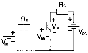
Fig. 3 - 2: Base biased CE
connection
Approximation: VBE = 0.7 V

Ex: Silicon Transistor
VBE = 0.7V, VBB =
10V, RB = 100 KW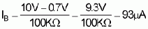
Collector curves (output)
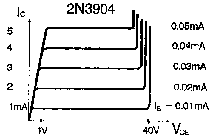
Fig. 3-3: NPN transistor collector
curve (2N3904)
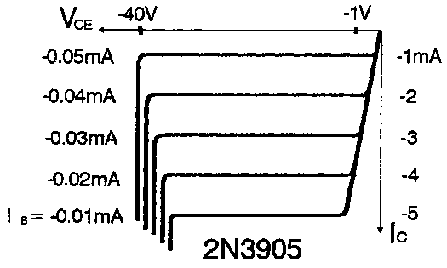
Fig. 3-4: PNP transistor collector
curve (2N3905)
Recall Kirchhoffs voltage law: (see Fig. 2-7)
VCE = VCC - IC * RC
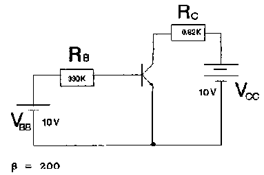
Ex: Analyse the following circuit
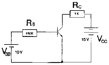
Fig. 3-5: Base biased CE
connection, b=100
IC = bdc * IB = 6.2 mA
VCE = VCC - IC * RC = 15V - (6.2 mA * 1 KW) = 8.8V
Regions of Operation
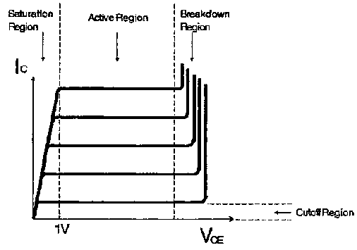
Fig. 3-5: Regions of operation
|
Active region : |
Normal operation |
|
Breakdown region: |
Transistor should never operate in this region |
|
Saturation region: |
VCE between 0V ----> 1V |
|
Cutoff region: |
IC approximately zero |
Transistor power dissipation
PD = VCE * IC
This power causes the junction temperature of the collector diode.
Important information from a data sheet:
Maximum power rating: PD (max.)
Transistor test
- Out of circuit: With an ohmmeter.
* resistance between collector and emitter should be high in both direction.
===> diodes are back to back in series (see also Fig. 2-3)
* reverse and forward resistance of emitter collector diode (reverse/forward ratio) should be more than 1000: 1 (silicon)
- In circuit: With a voltmeter
* measure VE and VC, the difference VE - VE should be more than 1V but less than VCC.
If VCE is less than
1V:----> transistor may
be shorted
If
VCE equals
VCC:---- >
transistor may be
open
Worksheet No. 3
Figure
No. 1 What is the base current ?
No. 2 If the current gain decreases from 200 to 100 what is the base current?
No. 3 What are the collector-emitter voltage and the transistor power dissipation?
No. 4 Suppose we connect a LED in series with the collector resistor. What does the LED current equal?
Experiment No. 3
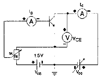
Figure
Procedure:
Adjust VCC in turn to every value of VCE shown in the table. Observe and record the value of IC for each value of VCE. Monitor IB, and readjust R1 if necessary.
From the data in the table, plot the collector characteristic curve (IC over VCE).
|
IB mA |
IC mA | ||||||||
| |
VCE volt | ||||||||
| |
0 |
2.5 |
5 |
7.5 |
10 |
15 |
20 |
25 |
30 |
|
10 | | | | | | | | | |
|
20 | | | | | | | | | |
|
30 | | | | | | | | | |
|
40 | | | | | | | | | |
|
50 | | | | | | | | | |
|
| ||||||||||||||||||||||||||||||||||||||||||||||||||||||||||||||||||||||||||||||||||||||||||||||||||||||
First Evaluation
No. 1 Define extrinsic semiconductor and intrinsic semiconductor.
No. 2 At room temperature an intrinsic silicon crystal acts approximately like a ..................
No. 3 The current in a transistor is split into parts. Which is the highest and how is it split?
No. 4 Please sketch the basic transistor connections.
No. 5 If the base current is 100 mA and the current gain is 30, what is the collector current?
No. 6 Sketch a typical set of collector curves, label the graph and mark the regions of operation.
No. 7 a) Please calculate the current gain b.
b)What is the voltage between collector and ground?

Figure
No. 8 Describe how you can find the base lead of an unknown transistor with the help of an ohmmeter.
|
| ||||||||||||||||||||||||||||||||||||||||||||||||||||||
Amplifier Teaching Aid (DED Philippinen, 86 p.)
Lesson 4 - Transistor Fundamentals
Lesson Plan
Title: Transistor Fundamentals
Objectives:
- Understand the meaning of load line and
Q-point
- Able to do the calculation for load line and Q-point
- Know the
principle of a transistor switch
Figure
The load line
The load line contains every possible operating point for the circuit. A line is defined by two points. To draw the load line you have to get. the saturation point and the cutoff point:
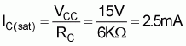
Saturation point: Tells you the maximum possible collector current for the circuit.
Calculate: Visualize a short between the collector and emitter.
VCE --- >
0
Cutoff point : Tells you the maximum possible collector emitter voltage for the circuit. Calculate: Visualize the transistor internally open between collector and emitter.
VCE -- > VCC
VCE (cut) = VCC
Ex: Draw the load line for the given circuit.
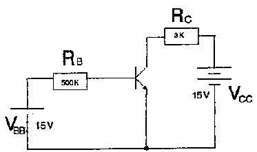
Fig. 4-1: CE amplifier base biased

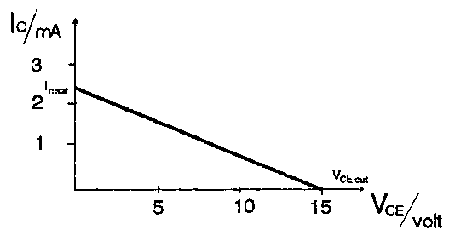
Fig. 4-2: Output curve
Saturation point:

Cutoff point:
VCE (cut) = VCC = 15V

Fig. 4-3: Output curve with loadline
HO: Suppose the collector resistance (in Fig. 4-1) is increased to 6KW. What happens to the dc load line?
Solution:
VCE (cut) = 15V
Figure
The operating point
Every transistor circuit has a load line. If the base resistance is given you can also calculate the current and voltage for the operating point.
Ex: Calculate the operating point (Q-point)

Fig. 4-4: Base biased CE
connection

IC = bdc * IB = 100 * 29mA = 2.9 mA
VCE = VCC - (IC * RC) = 15V - (2.9 mA * 3KW) = 6.3V
By plotting IC (2.9 mA) and VCE (6.3V), we get the operation point ----> Q-point (quiescent point).
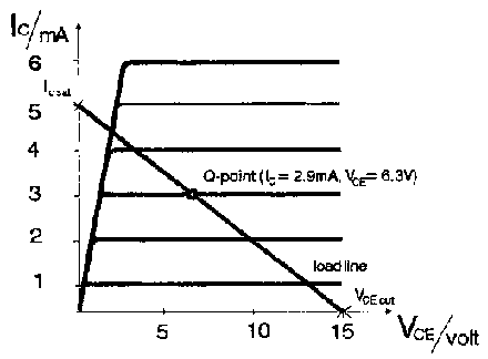
Fig. 4 - 5: Collector curve with
load line and Q - point
HO: Draw the load line and Q-point.

Fig. 4-6: base biased CE
connection, b=50
Solution:
IC = IB * b = 2.15 mA
VCE = VCC - (RC *
IC)= 5.7V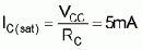
VCE (cut) = VCC = 3.0V

Figure
Recognizing saturation
When you first look at a transistor circuit, you usually cannot tell if it is saturated or operating in the active region.
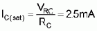
1. calculate IC (sat)
2. calculate IC
If IC is greater than IC (sat) the transistor is saturated.
Note: Current gain is less in saturation region.
The transistor switch
Ex: Circuit example for a transistor switch:
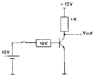
Fig. 4-7: Transistor switch
The transistor operate only at saturation and cutoff
Switch closed: Transistor in hard saturation Vout » 0V
Switch open : Transistor in
cutoffIC drops
to zero
Vout » 10V
Worksheet No. 4

Figure
No. 1 Draw the load line!
No. 2 If the collector resistance is increased to 1K, what happens to the load line?
No. 3 What is the voltage between the collector and ground if the current gain is 100?
|
| ||||||||||||||||||||||||||||||||||||
Amplifier Teaching Aid (DED Philippinen, 86 p.)
Lesson 5 - Transistor Biasing
Lesson Plan
Title: Transistor Biasing
Objectives:
- Understand the purpose of biasing
-
Able to analyze an emitter biased circuit
Figure
Transistor biasing
Emitter Bias
The analysis of base biased circuits depends on the current gain which can vary in a wide range. In an amplifier we need circuits whose Q-points are immune to changes in current gain. The solution for this problem is the emitter biased circuit:
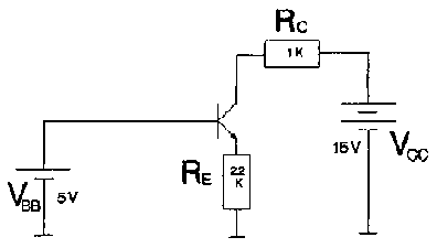
Fig. 5-1: Emitter biased circuit,
b = 100
Find the Q-point:
Given : VBB = 5V, VBE = 0.7V, VCE = 15V
RE = 2.2KW, RC = 1KW
Calculation:
VE = VBB -
VBE = 5V - 0.7V =
4.3V
IE = IC (close approximation)
VC = VCC - (RC *
IC)= 15V - (1KW - 1.95 mA)
=
13.1V
VCE =
VC - VE = 13.1V - 4.3V = 8.8V
Q-point coordinates:
IC = 1.95 mA
VCE = 8.8V
An emitter biased circuit is immune to changes in current gain. Analysing summary:
1. get VE
2. calculate
IE
3. find VC
4. VCE = VC - VE
At no time we need the current gain!
Tip for troubleshooter:
Don't measure direct VCE, because the common lead of the voltmeter is grounded, so you will short the emitter to ground.
1. Measure VC
2. Measure
VE
3. Subtract VCE = VC -
VE
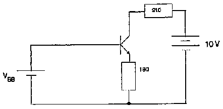
HO: What is the collector voltage?
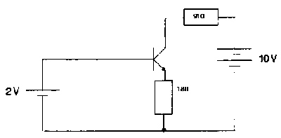
Fig. 5-2: Emitter biased CE
connection
Solution:
VE = VBB -
VBE = 2V - 0.7V =
1.3V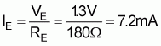
IE = IC (approx.)
VC = VCC - (RC * IC) = 10V - (910 W * 7.2 mA) = 3.4V
HO: What is the collector-emitter voltage?
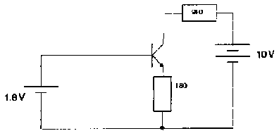
Fig. 5-3: Emitter biased CE
connection
Solution:
VE = VBB -
VBE = 1.1V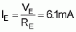
IE = IC (approx.)
VC = VCC - (RC * IC) = 9.4V
VCE = VC - VE = 8.35V
Effect of Small Changes
For example, tolerances of resistors (+/- 10%) are small changes.
See Fig. 5-4 on the next page.
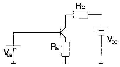
Fig. 5-4: Emitter biased CE
connection
Before we can analyse the effects of small changes we have to find out which values are dependent or independent.
independent values: VBB,
VCC, bdc, RE,
RC
dependent values : VE , VC,
IB, IC, IE
Suppose the independent values will increase one after another. What will be the effect on the dependent values:
|
increase |
dependent | ||||||
| |
|
VE |
IE |
IB |
IC |
VC |
VCE |
| |
VBB |
U |
U |
U |
U |
D |
D |
| |
VCC |
N |
N |
N |
N |
U |
U |
|
independent |
RE |
N |
D |
D |
D |
U |
U |
| |
RC |
N |
N |
N |
N |
D |
D |
| |
hfe |
N |
N |
D |
N |
N |
N |
U = up
D = down
N = no
change
Worksheet No. 5
Figure
No. 1 What is -the collector voltage if VBB = 2V?
No. 2 If the collector resistor is doubled, what is the collector emitter voltage for a base supply voltage of 2.3V?
No. 3 If the collector supply voltage is increased to 15V, what is the collector emitter voltage for VBB = 1.8V?
No. 4 The base supply voltage (2V) increases by 10%. What happens to the base current, collector current, and collector voltage?
|
| ||||||||||||||||||||||||||||||||||||||||||
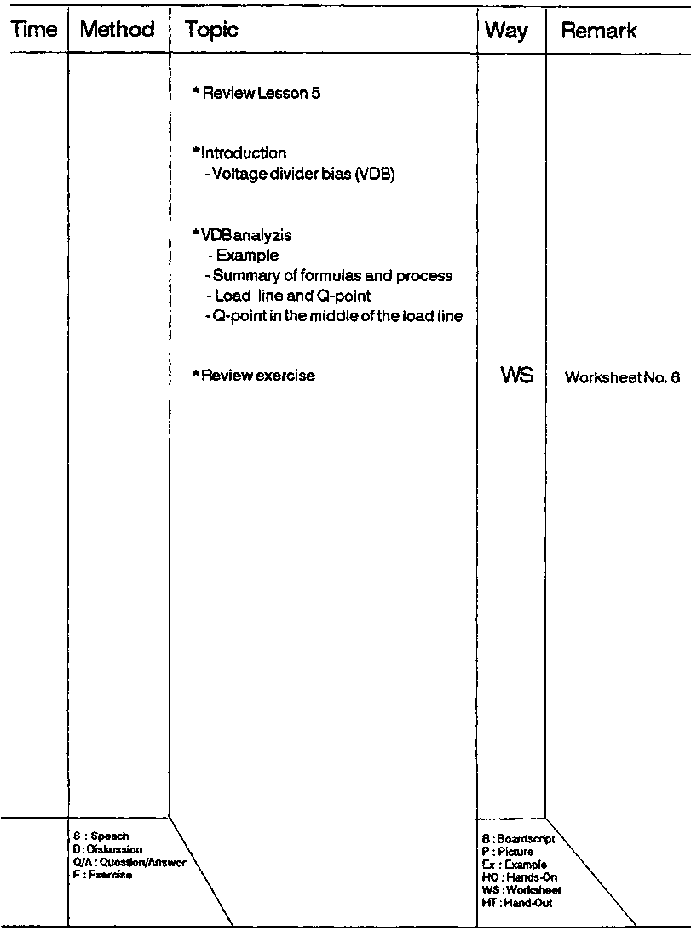
Amplifier Teaching Aid (DED Philippinen, 86 p.)
Lesson 6 - Transistor Biasing II
Lesson Plan
Title: Transistor Biasing II
Objectives:
- Know the advantage of voltage divider
bias
- Able to analyse VDB circuits
Figure
Transistor biasing II
Voltage Divider Bias
The most famous circuit based on -the prototype of emitter bias is called the voltage divider bias (VDB).
Recall the steps of analyzing the emitter bias circuit:
1. VE
2. IE
3.
IC
4. Voltage drop across RC
5. VC
6.
VCE
The three most important steps are:
1. IE
2. VC
3.
VCE

Fig. 6-1: Emitter biased
circuit
Problem: Sometimes the voltage from the VCC power supply is too large to apply directly at the base.
Solution:
- extra power supply for the base
- or
==> VDB
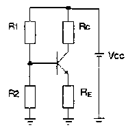
Fig. 6-2: VDB circuit
The voltage drop across R2 is applied directly to the base, which means:
V2 =
VB
1. step: find voltage drop across
R2
2. step: subtract 0.7V to get
VE
VDB analysis
Design errors of 5% or less are acceptable, because of resistor tolerances.
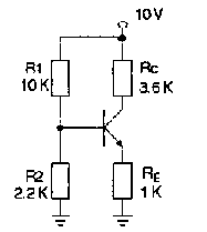
Fig. 6-3: VDB example circuit
Find the base voltage:
Assumption: Base current is so small that it has no effect on the voltage divider.
5% error - > base current is 20 times smaller than the divider current.
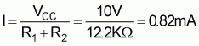
VB = I * R2 = 0.82 mA * 2.2KW = 1.8V
VE = VB - VBE = 1.8V - 0.7V =
1.1V
VC = VCC -(RC * IC) = 10V - (3.6KW * 1.1 mA) = 6.04V
VCE = VC - VE = 6.04V - 1.1V = 4.94V
Checking the assumption:
5% error --> 
The current gain can vary from 30 to
300.
Even under the worst case condition the calculation is within the 5% limit, hence the assumption can be done.
Summary of Process and Formulas
|
Divider current |
|
|
Base voltage |
VB = I * R2 |
|
Emitter voltage |
VE = VB - VBE |
|
Emitter current |
|
|
Collector voltage |
VC = VCC - (IC * RC) |
|
Coll.- emitter voltage |
VCE = VC - VE |


HO: What will change if the emitter resistor increases to 2KW? (unchanged voltage divider)
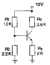
Fig. 6-4: VDB circuit
Solution:
I = 0.82 mA
VB = 1.8V
VE =
1.1V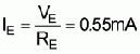
VC = VCC - (RC * IC) = 8.02V
VCE = VC - VE = 6.92V
VDB Load-Line and Q-Point
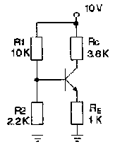
Fig. 6-5: VDB circuit
Saturation point:
Visualize short between collector and emitter
VRC = VCC - VE = 10V - 1.1V =
8.9V
- - > 
Cutoff point:
Visualize open between collector and emitter
- - > VCE (cut) = VCC - VE = 8.9V
Q-point:
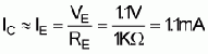
VC = VCC - (IC * RC) = 10V - (1.1 mA * 1KW) = 6.04V
VCE = VC - VE = 6.04V - 1.1V = 4.94V
Now we plot these values and get the load line and the Q-point:
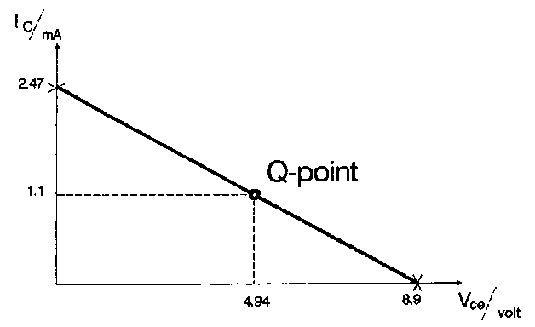
Fig. 6-6: Output curve with load
line and Q-point
The values VCC, RC, R1, and R2 are controlling saturation current and cutoff voltage. To move the Q-point is possible by varying the emitter resistance (RC).
Get the Q-point in the Middle of the Load Line
To set the Q-point is a important preparation as you will see later on.
Effect of RE:
RE too large -- > Q-point
moves into cutoff
RE too small --> Q-point moves into
saturation
Q - point in the middle of the load line:
Half the value of IC (sat) and redesign RE
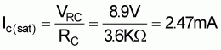
IC (sat) = 2.47 mA ==> 1.23
mA
Look for the nearest standard value:
===> 910 W

Fig. 6-7: Output curve, Q-point in
the
middle
Worksheet No. 6
Figure
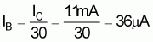
No. 1 What is -the emitter voltage? The collector voltage? Given: R1= 10k, R2= 2.2k, RC = 3.6k, RE = 1k, VCC = 25V
Draw the load-line, plot the Q point!
No. 2 What is the emitter voltage? The collector voltage?
Given: R1= 330k, R2= 100k, RC = 150k, RE = 51k, VCC = 10V
Draw the load-line, plot the Q point!
No. 3 What is the emitter voltage? The collector voltage? Given: R1 = 10k, R2 = 2.2k, RC = 2.7k, RE = 1k, VCC = 10V
Draw the load-line, plot the Q point!
Redesign the circuit to get the Q-point in the middle of the loadline!
|
| ||||||||||||||||||||||||||||||||||||||||||||||||||||||||||||||||||||||||||||||||||||||||||||||||||||||
Second Evaluation
No. 1 If the base resistor is very small, -the -transistor will operate in the a. cutoff region b. active region c. saturation region d. breakdown region
No. 2 If a transistor operates in the middle of the load line, an increase in the base resistance will move the Q-point a. up b. down c. nowhere d. off the load line
No. 3 The saturation point is approximately the same as a. cutoff point b. lower end of the load line c. upper end of the load line
No. 4 When the collector resistance decrease in a base biased circuit, the load line becomes a. more horizontal b. more vertical c. fixed
No. 5 The first step in analyzing emitter biased circuits is to find the a. base current b. emitter voltage c. emitter current d. collector current
No. 6 If the emitter resistance decreases, the collector voltage a. decreases b. stays the same c. increases d. breaks down the transistor
No. 7 If the emitter resistance doubles in a VDB circuit, the collector current will a. double b. drop in half c. remain the same d. increase
No. 8
a) What is the emitter voltage?
b) The collector voltage?
c) Draw the load line, plot the Q-point!
d) Redesign the circuit to get the Q-point in the middle of the load line.
Given: R1 = 12KW, R2 = 3KW, RC = 3.2 KW, RE = 1KW, VCE = 10V
Figure
|
| ||||||||||||||||||||||||||||||||||||||||||||||||||||||||||||
Amplifier Teaching Aid (DED Philippinen, 86 p.)
Lesson 7 - Small Signal Amplifier
Lesson Plan
Title: Small Signal Amplifier
Objectives:
- Know the purpose of capacitors in
amplifier circuits
- Able to calculate the voltage gain in an CE
amplifier
Figure
Small signal amplifier
AC Signals
After the transistor has been biased with the Q-point near the middle of the load line, we can put a small ac-voltage on the base (Vin). That procedures a large ac voltage at the collector (Vout). This increase is called amplification. For two reasons we have to use capacitors. First, to couple or transmit ac signals (coupling). Second, to short ac signals to ground (bypass).
Coupling capacitor
A capacitor is open at low frequencies and shorted at high frequencies.
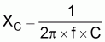
Capacitive reactance (XC) is inversely proportional to frequency (f) and to capacitance (C). For a coupling capacitor to work properly, it has to act like an ac short at the lowest frequency that the ac source can have. To realize that we can use the following rule:
XC < 10 R
Make the reactance at least 10 times smaller than the total resistance in series with the capacitor.
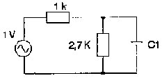
Ex: Calculate the capacitance of C1 for a proper ac transmittance. Frequency range: 20-20000 Hz

Fig. 7-1: Use of coupling
capacitor
Total resistance: 1KW + 500W = 1.5KW
XC <= 10 * R -- >
 -- >
-- > 
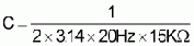
C = 53mF
The capacitor to choose should be bigger than 53mF. The next standard value is:
C = 56mF
Bypass capacitor
It is connected in parallel across a resistor. The reason for doing this is to bypass an ac current away from the resistor. The capacitor provides a short for the ac. You can use the following rule to calculate the capacitance:
Make the reactance at least 10 times smaller than the total resistance in parallel with the capacitor.
Amplifier analyzing method
From a given amplifier circuit first do -the dc analysis (recall lesson 6) and than do the ac analysis.

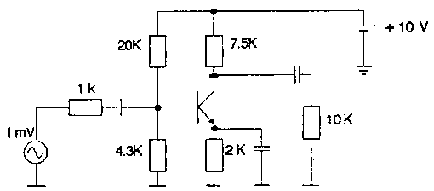
Fig. 7-2: CE amplifier circuit
DC equivalent circuit
For dc, all capacitors are acting like open switches; therefore we can draw the following dc equivalent circuit:

Fig. 7-3: DC equivalent
circuit
Now the dc analysis can easily be done: (see Lesson 6)
VB = 1.8V
VE =
1.1V
IE = 1.1 mA
VC = 6.04V
VCE =
4.94V
AC equivalent circuit
For the ac all capacitors are shorted and the dc sources are reduced to zero:
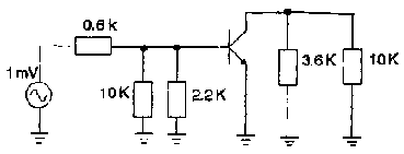
Fig. 7-4: Ac equivalent,
circuit
The top of the 10K and 3.6K resistors are grounded. The resistors 10K/2.2K and 3.6K/10K are in parallel so we can combine them:
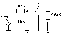
Fig. 7-4: Simplified ac equivalent
circuit
Now we got a really simple circuit for the ac analysis.
Voltage Gain
One of the most important characteristics for small signal amplifiers is the voltage gain (AV).

The lowercase letters are used to indicate ac values. The output voltage is given by:
Vout = ic * rc
The input voltage is given by:
Vin = ie * re
Substitute of these two expressions:

Because ic approximately equals ie:

AC emitter resistance (re)
The first step in calculating the voltage gain is to estimate the ac emitter resistance (re).
 (formula
derived by using calculus)
(formula
derived by using calculus)
This relation applies to all transistors that means it is a universal formula.
Let's remember our example circuit (Fig. 7-4):
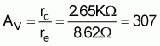
AC collector resistance
Due to the ac analyzing method we easily get the ac collector resistance (re). See Fig. 7-4:
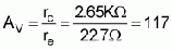
rc = 2.65KW
So now we are ready to calculate the voltage gain:
HO: What will be the voltage gain for the following circuit?
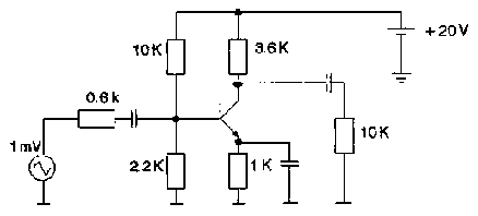
Fig. 7-5: CE amplifier circuit
Solution:
DC analysis
VB = 3.6KW, VE = 2.9 KW, IE = 2.9 mA
VC = 9.5V, VCE = 6.6V
AC analysis
rc = 2.65KW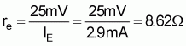
Worksheet No. 7
Figure
No. 1 (circuit above) Calculate the capacitance of C1, to design a proper working bypass capacitor for the load RL. Frequency range: 20 - 20000 Hz
No. 2 (circuit below)
a) Draw the dc equivalent circuit.
b)
Calculate the following dc values: IC, VCE
c) Draw the
ac equivalent circuit.
d) Calculate the ac emitter resistance (re)
and the ac collector resistance (rc).
e) What is the voltage gain
AV?
f) What happens to the voltage gain if the supply voltage
doubles?
Figure
Experiment No. 4

Figure
Procedure:
1. Connect the circuit
2. Connect an signal generator to the input. Set it to 1000 Hz (sinewave) and minimum output. Connect an oscilloscope to the output terminals of the amplifier. Adjust the oscilloscope for proper viewing.
3. Set the output of the generator to the maximum undistorted
amplifier output.
Measure the peak to peak input and output amplitude and
record it in the table. Draw the input and output waveforms in the table.
4. Set the generator to the minimum undistorted amplifier
output.
Measure the peak to peak input and output amplitude and record it in
the table. Sketch the input and output waveforms in the table.
|
Step |
|
Input |
Output | ||
| |
IC |
Vp-p |
Waveform |
Vp-p |
Waveform |
|
3 | | | | | |
|
4 | | | | | |
|
| ||||||||||||||||||||||||||||||||||||||||||||||||||||||
Amplifier Teaching Aid (DED Philippinen, 86 p.)
Lesson 8 - Small Signal Amplifier II
Lesson Plan
Title: Small Signal Amplifier II
Objectives:
- Able to calculate the input
impedance
- Understand the purpose of impedance matching

Figure
Signals in a CE amplifier
One characteristic of the CE amplifier is the phase inversion.
See Handout No. 1 (let the students complete)
For a better understanding the different voltage signals are plotted in four graphs:
Graph 1: A small ac signal is applied at
the amplifier input.
Graph 2: The small ac signal is topping the biasing
dc.
Graph 3: The amplified and inverted ac signal is topping the biasing
dc.
Graph 4: The output capacitor C2 is blocking the dc, the
amplified inverted ac signal is applied at the
load.
Input impedance
Another important value to analyze is the input impedance of an amplifier circuit.
Recall the ac equivalent circuit in Lesson 7:
(see Fig. 8-1 on the next page)

Fig. 8-1: AC equivalent circuit
RG is equal to the internal resistance of the signal source. Input impedance looking into the base:

ie/ib is approximately equal to b:
zb = b * re
The input impedance of a amplifier stage is the combination of base impedance and biasing resistance:
zin = R1//R2//b * re
Ex: What is the input impedance in Fig. 8-1?
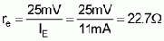
re = 22.7 W, b = 100
zin = 1.8 KW//22.7
W *
100
= 202 W
Impedance matching
When you couple some amplifier stages or connect electronic appliances, the input/output impedance of every stage will effect the efficiency.

Fig. 8-2: Impedance matching
The internal resistance/impedance of the signal source (R1) and the loudspeaker (R4) is fixed. Only R2 and R3 can be designed to match the impedance.
Voltage optimum
Between signal source and amplifier it is important to transfer the highest possible voltage.

Fig. 8-3: Voltage optimum

In order to get the highest, possible voltage (V2) let's try several values for R2.
Ex: V = 10V, R1 = 100 W
R2 = 0.1 *
R1 --- > 
R2 = R1 ---
> 
R2 = 10 * R1
--- > 
R2 = 100 * R1
--- > 
The input impedance of an amplifier should be much bigger than the internal resistance of the signal source.
Power Optimum
Between amplifier and loudspeaker it is most important to transfer the highest possible power.

Fig. 8-4: Power optimum
Ex: Power in the load under different values of R4.
V = 10V, R3 = 8W PL = R4 *
I2
PL = R4 *
I2
|
R4 = 16W |
I = 24W = 0.42A |
PL = 2.78W |
| | | |
|
R4 = 8W |
I = 16W = 0.63A |
PL = 3.125W |
| | | |
|
R4 = 4W |
I = 12W = 1.14A |
PL = 1 .03W |
Input impedance of the load and the output impedance of the amplifier should have the same value.
R3 = R4
Ri = RL
Handout No. 1

Figure
Worksheet No. 8

Figure
No. 1 a) The generator voltage doubles. What is the input impedance?
b) The generator resistance RG doubles. What is the input impedance?
No. 2 You like to connect a microphone (R = 100KW) to an amplifier. What should be the input impedance of the amplifier to get a voltage optimum?
Microphone output voltage Vout = 10 mV
No. 3 The output impedance of your amplifier is 6W. What kind of loudspeaker (4W or 8W) do you choose to get the best power transfer?
|
| ||||||||||||||||||||||||||||||||||||||||||||||||||||||
Amplifier Teaching Aid (DED Philippinen, 86 p.)
Lesson 9 - Small Signal Amplifier III
Lesson Plan
Title: Small Signal Amplifier III
Objectives:
- Know the characteristics of CE, CB, and
CC configurations
- Understand why the output voltage depends on the
frequency
- Able to construct the ac load line

Figure
Other configurations
Up to now we discussed only the common emitter configuration, which is widely used. But for some circuit conditions the common base or the common collector configuration may be a better choice.
As we had already seen, the input/output impedance of an amplifier is a very important characteristic, because the internal impedance of signal sources vary widely:
Ex:
Antenna --- > approx. 50 W
Microphone --- > approx. 100000 W
To choose the best configuration let's have a look at its characteristics.
See Handout No. 2 (let the students complete)
Common base CB
- High voltage gain
- No current
gain
- Low input impedance
- High output impedance
- No phase
inversion
Common collector CC
- No voltage gain
- High current
gain
- High input impedance
- Low output impedance
- No phase
inversion
Common emitter CE
- High voltage gain
- High current
gain
- Medium input impedance
- Medium output impedance
- Phase
inversion
Frequency response of an amplifier

Fig. 9-1: Amplifier output voltage
in terms of frequency
Fig. 9-1 shows the typical frequency response of an amplifier. At low frequencies the output voltage decreases because of coupling and bypass capacitors. At high frequencies, the output voltage decreases because of transistor and stray wiring capacitance.
Critical frequencies:
Where the output voltage is 0.707 of
Vmax.
Two critical frequencies -> f1,
f2
Midband:
Is the band of frequencies between 10 *
f1 and 0.1 * f2.
The midband is where an amplifier is
supposed to be operated.
Ex: Find the midband of an amplifier with f1 = 5 Hz and f2 = 100 KHz.
10 * f1 = 10 * 5 Hz = 50 Hz -- > lower end
0.1 * f2 = 0.1 * 100 KHz = 10 KHz -- > upper end
Midband: 50 Hz - 10 KHz
The AC load line
In previous lessons we used the dc load line to analyze biasing circuits. But an amplifier sees two loads, a dc load and a ac load. Now we will use the ac load line to understand the large signal operations.

Fig. 9-2: CE amplifier
DC values: VB = 1.8V, VE = 1.1V, IE = 1.1 mA, VC = 6.04V VCC = 10V, VCE = 4.94V
Without load: DC an ac load line are the same.
With load: rc = RC//RL

AC Load Line Construction
The following process shows you an easy method to get the ac load line:
1. Draw the dc load line
VCE (cut) = VCC - VE = 8.9V
2. Calculate and draw the Q point
IC = 1.1 mA
VCE = 6.04V
3. Draw a -temporary ac load line
VCE (cut) =
VCC
4. Construct the ac load line
- parallel to the temporary ac load
line
- passing the Q point

Fig. 9-3: Construction of an ac
load
line
Handout No. 2

Figure
Worksheet No. 9
No. 1 An amplifier has -this critical frequencies:
f1 = 2 Hz, f2 = 200 KHz
What is the midband?
No. 2 See Worksheet No. 8, Problem No. 3.
What kind of transistor connection would you choose for the first stage of the amplifier? Explain!
No. 3 Construct the ac load line for the following circuit.

Figure
|
| ||||||||||||||||||||||||||||||||||||||||||||||||||||||||||||
Amplifier Teaching Aid (DED Philippinen, 86 p.)
Lesson 10 - Large Signal Amplifier
Lesson Plan
Title: Large Signal Amplifier
Objectives:
- Understand the importance of amplifier efficiency
- Know
the most common classes of power amplifier and their basic characteristics

Figure
Large signal amplifier
The early stages of amplifier systems are dealing with small signals. These stages are designed to give good voltage gain. Small signal transistors have a power rating of less than half a watt and power transistors have a power rating of more than half a watt.
The later stages of an amplifier system have much larger collector currents, because the load impedances are much smaller (i.e.: Loudspeaker 1W, 4W, 8W, 16W).
Efficiency is most important when large amounts of signal power are required:
Classes
This refers to how the amplifying device is biased. Amplifier can be biased for class A, B or AB operation.
Class A power amplifier
The amplifiers we have discussed have been class A amplifiers. Class A amplifier operate in the center of the load line. This gives the best possible output swing without clipping.
Efficiency: low, maximum 50%
Even when no signal is applied, a high current is flowing (100 mA) and there is a power dissipation in the load.
Distortion: low
Applications: Few audio amplifier (high quality)

Fig. 10-1: Class A
amplifier
Class B power amplifier
The class B amplifier is biased at cutoff. No current will flow until an input signal provides the bias to turn on the amplifier.

Fig. 10-2: Q point of a class B
amplifier
Only one half of the input signal is amplified. Two transistors can be operate in class B together in one circuit, one transistor for the positive portion of the signal and one transistor for the negative portion of the signal (Push Pull):

Fig. 10-3: Push Pull amplifier
Fig. 10-4: Signal swing of a. push
pull amplifier, Class B operation
Problem: Crossover distortion, the emitter diode takes 0,7V to turn on.

Fig. 10-5: Crossover
distortion
Efficiency: 78.5%
Distortion: High
Application: High power stages, not used in audio applications.
Class AB power amplifier
Solution to the crossover distortion:
Provide some forward bias for the base emitter junction.
Fig. 10-6: Class AB amplifier
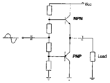
Fig. 10-7: Complementary push pull
amplifier
Two complementary transistors are used (NPN + PNP) , so no transformer is needed any more.
Efficiency: between A and B
Distortion: Moderate
Application: High power stages in audio and radio-frequency applications.
Worksheet No. 10
No. 1 Explain the difference between class A and class B power operation.
No. 2 Draw a circuit of a complementary push pull amplifier.
No. 3 Why is the efficiency of a class A power amplifier so low?
No. 4 In the graph below you see the Q points of different power amplifiers. Which Q point belongs to which type of power amplifier?
Label the graph!

Figure
|
| ||||||||||||||||||||||||||||||||||||||||||||||||||||||||||||||||||||||||||||||||||||||||||||||||||||||
Third Evaluation
No. 1 Characteristic parameter of -the transistor connections. Fill in: yes/no/high/low/medium
| |
common base |
common collector |
common emitter |
|
voltage gain |
| | |
|
current gain |
| | |
|
input impedance |
| | |
|
output impedance |
| | |
|
phase inversion |
| | |
No. 2
a) What is the voltage gain
AV?
b) What is the input impedance?
c) Construct the ac load
line!

Figure
No. 3 a) What are the classes of power amplifiers? Discuss advantage and disadvantage of every class.
b) Sketch a circuit of a push pull amplifier.